1/9
March 2001
STP70NF03L
STB70NF03L-1
N-CHANNEL 30V - 0.008
- 70A TO-220/I
2
PAK
LOW GATE CHARGE STripFETTM POWER MOSFET
(1) I
SD
70A, di/dt
290A/µs, V
DD
=24 V ; T
j
T
JMAX.
s
TYPICAL R
DS
(on) = 0.008
s
TYPICAL Q
g
= 35 nC @ 10 V
s
OPTIMAL R
DS
(on) x Q
g
TRADE-OFF
s
CONDUCTION LOSSES REDUCED
s
SWITCHING LOSSES REDUCED
DESCRIPTION
This application specific Power Mosfet is the third
generation of STMicroelectronics unique "Single
Feature Size
TM"
strip-based process. The result-
ing transistor shows the best trade-off between on-
resistance and gate charge. When used as high
and low side in buck regulators, it gives the best
performance in terms of both conduction and
switching losses. This is extremely important for
motherboards where fast switching and high effi-
ciency are of paramount importance.
APPLICATIONS
s
SPECIFICALLY DESIGNED AND OPTIMISED
FOR HIGH EFFICIENCY CPU CORE DC/DC
CONVERTERS
ABSOLUTE MAXIMUM RATINGS
(
q
) Pulse width limited by safe operating area
TYPE
V
DSS
R
DS(on)
I
D
STP70NF03L
STB70NF03L-1
30 V
30 V
< 0.01
< 0.01
70 A
70 A
Symbol
Parameter
Value
Unit
V
DS
Drain-source Voltage (V
GS
= 0)
30
V
V
DGR
Drain-gate Voltage (R
GS
= 20 k
)
30
V
V
GS
Gate- source Voltage
± 15
V
I
D
Drain Current (continuos) at T
C
= 25∞C
70
A
I
D
Drain Current (continuos) at T
C
= 100∞C
50
A
I
DM
(
q
)
Drain Current (pulsed)
280
A
P
TOT
Total Dissipation at T
C
= 25∞C
100
W
Derating Factor
0.67
W/∞C
dv/dt (1)
Peak Diode Recovery voltage slope
4
V/ns
T
stg
Storage Temperature
≠65 to 175
∞C
T
j
Max. Operating Junction Temperature
175
∞C
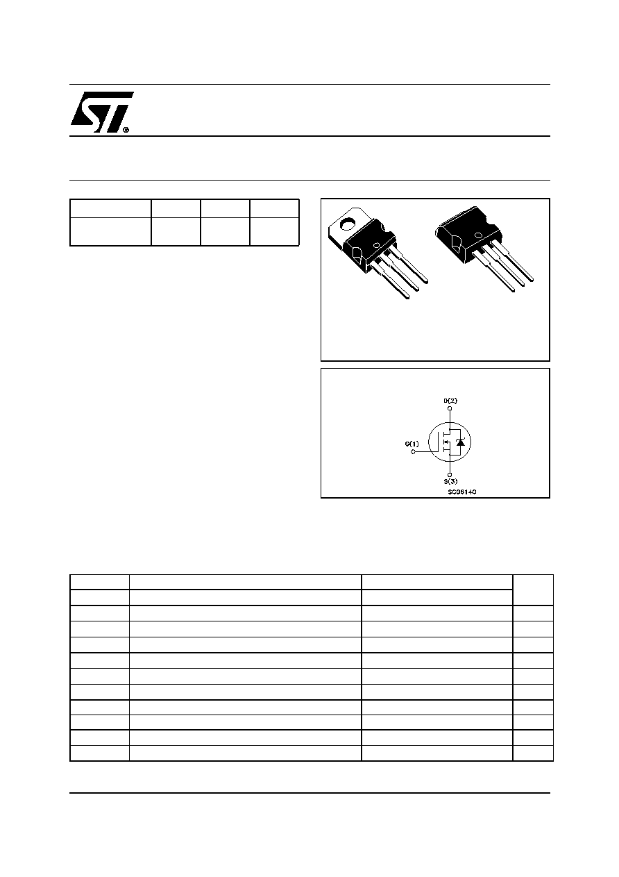
TO-220
1
2
3
1
2
3
I
2
PAK
INTERNAL SCHEMATIC DIAGRAM
STP70NF03L/STB70NF03L-1
2/9
THERMAL DATA
AVALANCHE CHARACTERISTICS
ELECTRICAL CHARACTERISTICS (TCASE = 25 ∞C UNLESS OTHERWISE SPECIFIED)
OFF
ON
(1)
DYNAMIC
Rthj-case
Thermal Resistance Junction-case Max
1.5
∞C/W
Rthj-amb
Thermal Resistance Junction-ambient Max
62.5
∞C/W
T
l
Maximum Lead Temperature For Soldering Purpose
300
∞C
Symbol
Parameter
Max Value
Unit
I
AR
Avalanche Current, Repetitive or Not-Repetitive
(pulse width limited by T
j
max)
35
A
E
AS
Single Pulse Avalanche Energy
(starting T
j
= 25 ∞C, I
D
= I
AR
, V
DD
= 50 V)
450
mJ
Symbol
Parameter
Test Conditions
Min.
Typ.
Max.
Unit
V
(BR)DSS
Drain-source
Breakdown Voltage
I
D
= 250 µA, V
GS
= 0
30
V
I
DSS
Zero Gate Voltage
Drain Current (V
GS
= 0)
V
DS
= Max Rating
1
µA
V
DS
= Max Rating, T
C
= 125 ∞C
10
µA
I
GSS
Gate-body Leakage
Current (V
DS
= 0)
V
GS
= ± 15V
±100
nA
Symbol
Parameter
Test Conditions
Min.
Typ.
Max.
Unit
V
GS(th)
Gate Threshold Voltage
V
DS
= V
GS
, I
D
= 250µA
1
2
V
R
DS(on)
Static Drain-source On
Resistance
V
GS
= 10 V, I
D
= 35 A
0.008
0.01
V
GS
= 5 V, I
D
= 18 A
0.015
0.018
I
D(on)
On State Drain Current
V
DS
> I
D(on)
x R
DS(on)max,
V
GS
= 10V
70
A
Symbol
Parameter
Test Conditions
Min.
Typ.
Max.
Unit
g
fs
(1)
Forward Transconductance
V
DS
> I
D(on)
x R
DS(on)max,
I
D
= 35 A
40
S
C
iss
Input Capacitance
V
DS
= 25V, f = 1 MHz, V
GS
= 0
1470
pF
C
oss
Output Capacitance
490
pF
C
rss
Reverse Transfer
Capacitance
110
pF
3/9
STP70NF03L/STB70NF03L-1
ELECTRICAL CHARACTERISTICS (CONTINUED)
SWITCHING ON
SWITCHING OFF
SOURCE DRAIN DIODE
Note: 1. Pulsed: Pulse duration = 300 µs, duty cycle 1.5 %.
2. Pulse width limited by safe operating area.
Symbol
Parameter
Test Conditions
Min.
Typ.
Max.
Unit
t
d(on)
Turn-on Delay Time
V
DD
= 15 V, I
D
= 35 A
R
G
= 4.7
V
GS
= 4.5 V
(see test circuit, Figure 3)
20
ns
t
r
Rise Time
350
ns
Q
g
Total Gate Charge
V
DD
= 24 V, I
D
= 46A,
V
GS
= 10V
35
45
nC
Q
gs
Gate-Source Charge
5
nC
Q
gd
Gate-Drain Charge
10
nC
Symbol
Parameter
Test Conditions
Min.
Typ.
Max.
Unit
t
d(off)
Turn-off-Delay Time
V
DD
= 15 V, I
D
= 35 A,
R
G
= 4.7
,
V
GS
= 4.5V
(see test circuit, Figure 3)
35
ns
t
f
Fall Time
65
ns
Symbol
Parameter
Test Conditions
Min.
Typ.
Max.
Unit
I
SD
Source-drain Current
70
A
I
SDM
(1)
Source-drain Current (pulsed)
280
A
V
SD
(2)
Forward On Voltage
I
SD
= 70 A, V
GS
= 0
1.5
V
t
rr
Reverse Recovery Time
I
SD
= 70 A, di/dt = 100A/µs,
V
DD
= 20 V, T
j
= 150∞C
(see test circuit, Figure 5)
75
ns
Q
rr
Reverse Recovery Charge
110
nC
I
RRM
Reverse Recovery Current
2.9
A
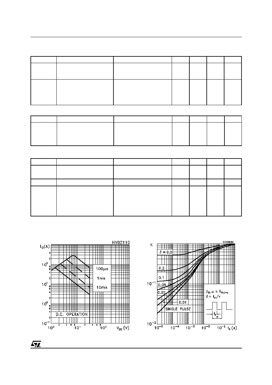
Thermal Impedence
Safe Operating Area
STP70NF03L/STB70NF03L-1
4/9
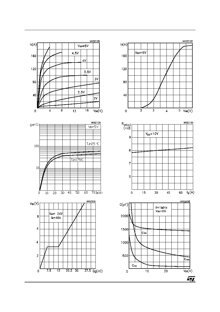
Gate Charge vs Gate-source Voltage
Transfer Characteristics
Output Characteristics
Transconductance
Static Drain-source On Resistance
Capacitance Variations
5/9
STP70NF03L/STB70NF03L-1
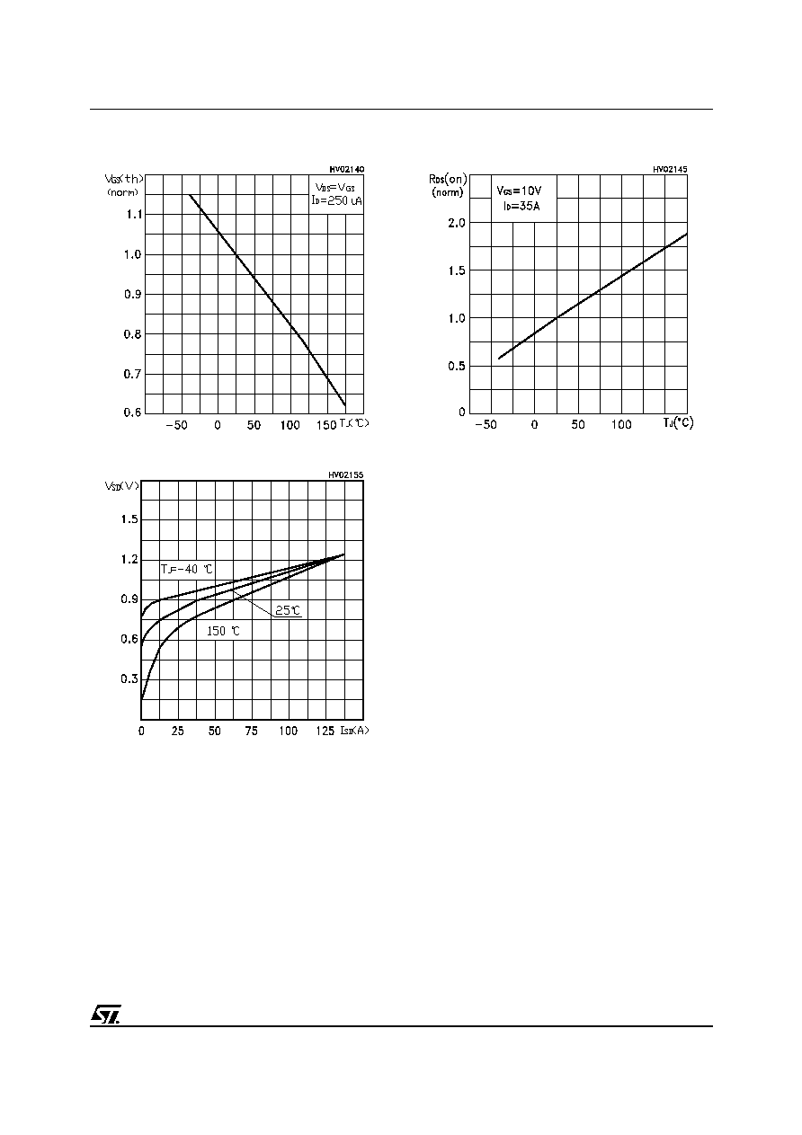
Normalized Gate Threshold Voltage vs
Temperature
Source-drain Diode Forward Characteristics
Normalized On Resistance vs Temperature
STP70NF03L/STB70NF03L-1
6/9
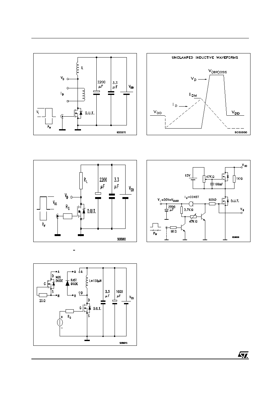
Fig. 5: Test Circuit For Inductive Load Switching
And Diode Recovery Times
Fig. 4: Gate Charge test Circuit
Fig. 2: Unclamped Inductive Waveform
Fig. 1: Unclamped Inductive Load Test Circuit
Fig. 3: Switching Times Test Circuit For
Resistive Load
7/9
STP70NF03L/STB70NF03L-1
DIM.
mm
inch
MIN.
TYP.
MAX.
MIN.
TYP.
MAX.
A
4.40
4.60
0.173
0.181
C
1.23
1.32
0.048
0.051
D
2.40
2.72
0.094
0.107
D1
1.27
0.050
E
0.49
0.70
0.019
0.027
F
0.61
0.88
0.024
0.034
F1
1.14
1.70
0.044
0.067
F2
1.14
1.70
0.044
0.067
G
4.95
5.15
0.194
0.203
G1
2.4
2.7
0.094
0.106
H2
10.0
10.40
0.393
0.409
L2
16.4
0.645
L4
13.0
14.0
0.511
0.551
L5
2.65
2.95
0.104
0.116
L6
15.25
15.75
0.600
0.620
L7
6.2
6.6
0.244
0.260
L9
3.5
3.93
0.137
0.154
DIA.
3.75
3.85
0.147
0.151
L6
A
C
D
E
D1
F
G
L7
L2
Dia.
F1
L5
L4
H2
L9
F2
G1
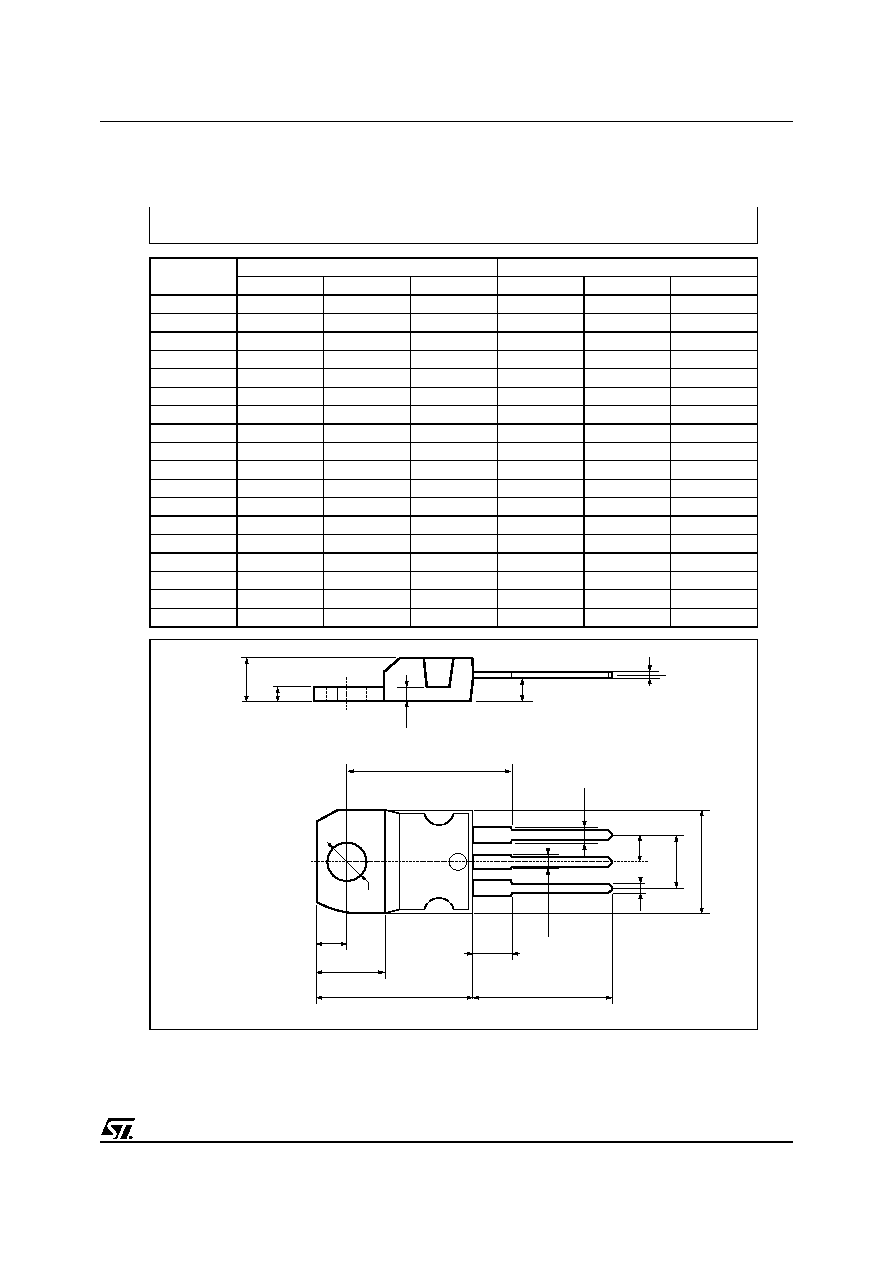
TO-220 MECHANICAL DATA
P011C
STP70NF03L/STB70NF03L-1
8/9
DIM.
mm
inch
MIN.
TYP.
MAX.
MIN.
TYP.
MAX.
A
4.4
4.6
0.173
0.181
A1
2.49
2.69
0.098
0.106
B
0.7
0.93
0.027
0.036
B2
1.14
1.7
0.044
0.067
C
0.45
0.6
0.017
0.023
C2
1.23
1.36
0.048
0.053
D
8.95
9.35
0.352
0.368
e
2.4
2.7
0.094
0.106
E
10
10.4
0.393
0.409
L
13.1
13.6
0.515
0.531
L1
3.48
3.78
0.137
0.149
L2
1.27
1.4
0.050
0.055
L
L1
B2
B
D
E
A
C2
C
A1
L2
e
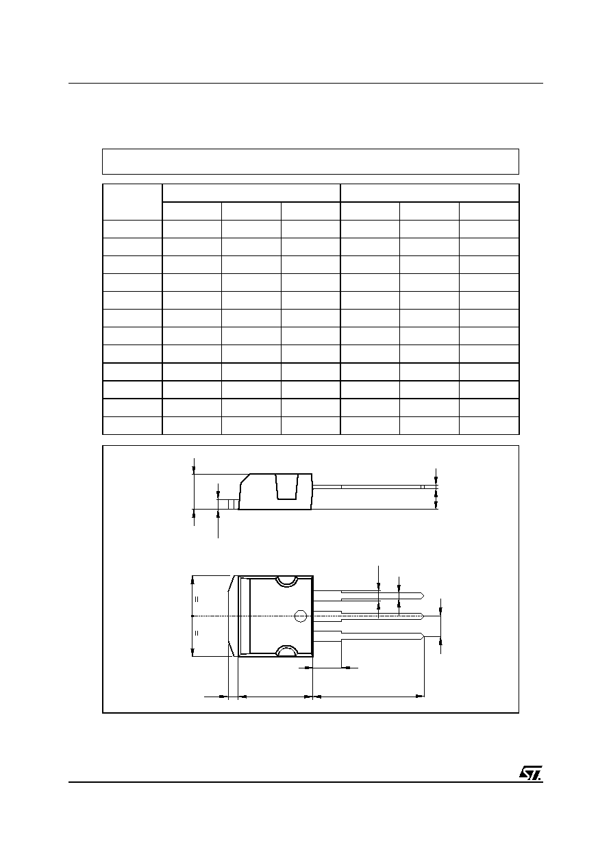
P011P5/E
TO-262 (I
2
PAK) MECHANICAL DATA

9/9
STP70NF03L/STB70NF03L-1
Information furnished is believed to be accurate and reliable. However, STMicroelectronics assumes no responsibility for the consequences
of use of such information nor for any infringement of patents or other rights of third parties which may result from its use. No license is
granted by implication or otherwise under any patent or patent rights of STMicroelectronics. Specification mentioned in this publication are
subject to change without notice. This publication supersedes and replaces all information previously supplied. STMicroelectronics products
are not authorized for use as critical components in life support devices or systems without express written approval of STMicroelectronics.
The ST logo is a trademark of STMicroelectronics
© 2000 STMicroelectronics ≠ Printed in Italy ≠ All Rights Reserved
STMicroelectronics GROUP OF COMPANIES
Australia - Brazil - China - Finland - France - Germany - Hong Kong - India - Italy - Japan - Malaysia - Malta - Morocco -
Singapore - Spain - Sweden - Switzerland - United Kingdom - U.S.A.
http://www.st.com